SJTU ACM Class Architecture 2021 Assignment ( MS108 Course Project )
[origin repo][https://github.com/ACMClassCourses/RISCV-CPU]
For feature details, please refer to project report.
| Feature | Status |
|---|---|
| Simulation Correct Output | Test OK |
| FPGA Correct Output | Test OK |
| Data Forwarding to avoid stall | Test OK |
| ICache ( direct mapping)(128 entry) | Test OK |
| DCache (Write through&&write allocate*) (32 entry direct mapping) | Test OK |
| 32 entry BTB (branch target buffer )while every entry has 1 bit BHT(branch history table)* | Test OK |
| Read Priority over Write on Miss*(dcache write buffer *maxmize the bus use rate using circular queue) | Test OK |
| naive mmu | |
| IF Prefetch |
*while the btb can branch in the pc stage instead of ex stage which save 3 cycle the bht gurantee the currectness
*Write allocate: allocate new cache line in cache
*write buffer is an optimizen of write through in the dcache
*when the load occur we examine the wrie buffer to find if the data exist in the write buffer(using circular queue )
the best result at the frequence of 100HZ(higher frequence should be tested)
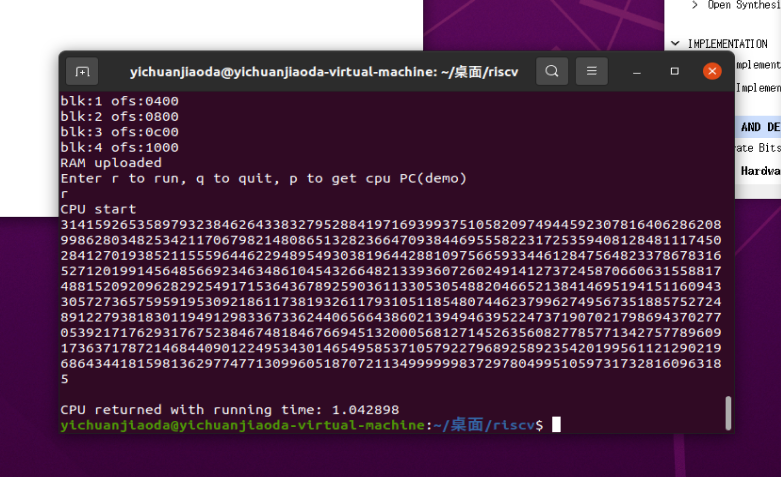
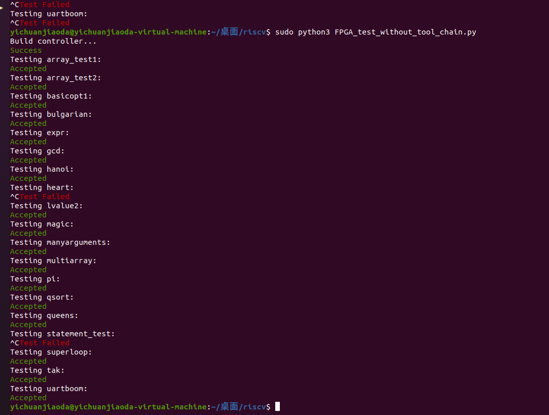
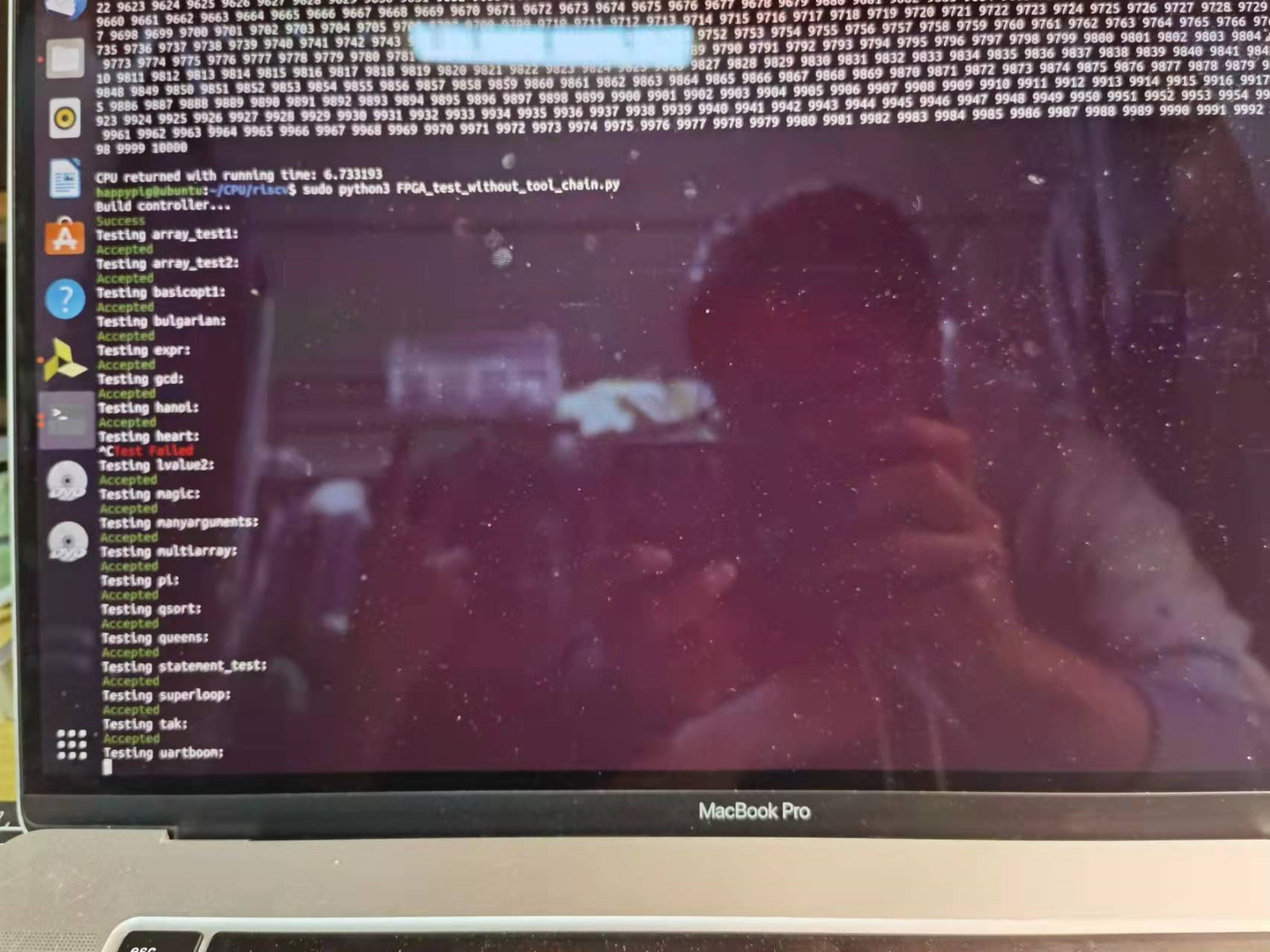
all test result (note that the statement_test need to be programed again due to the problem issued in fpga )
(the heart testcase take such time and I put the result in the above)
- about write buffer
The motivation for Write Buffer : The memory port on FPGA is completely different from RAM in modern computer, where the motivation for Write Buffer comes from. Write Buffer dalays unimportant write behavior to gaps between reading.when the bus is spare it can be reused to store the data in the write buffer into the ram.
and when I design this unit I meet a problem that trouble me a few days, that''s because when i first design the write buffer I simply use the sequeint array so when the load instruction want a data in the write buffer the write buffer may has two entry having the same data address but different data so I can't get the correct one.So in my design ,I use a method like circuit quene so I can get the latest data in the write bufferto guarantee correctness.
- about dcache
A direct mapping D-Cache with size of
In my [pre_commit][https://github.com/yichuan520030910320/CPU_ACM_2021/commit/0d435f14a7e02868a939453481c9623ef4f2bcc6] I adopt a write back dcache the write policy is a mixture of write back and write through, and in detail, 4-byte store insructions use write back and other store instructions use write through. It is so arranged because of the large proportion of 4-byte store instructions, and the 4-byte block size due to limitation of units on FPGA.
it can correctly run the simulation but due to the complex design the latency in the fpga is such big .So I uphold the principle
"Small is fast, simple and neat, good design is a good trade-off" in the Bible. I change the design into write through&&write allocate and make the dache It can always make the cache the same as ram.Just simple but effective.
- about BHT&BTB
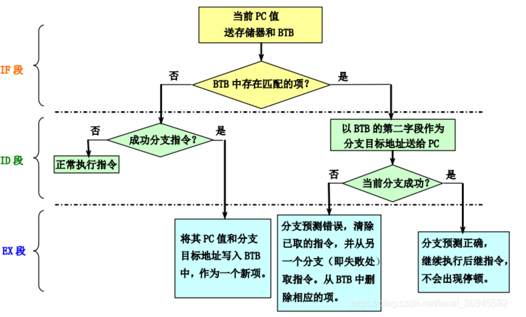
the outline design of btb is the same as the below
but it can't guarantee the correctness so I adopt one bit bht to check if the instruction jump
| 33 | 32:15 | 14:2 | 1:0 |
|---|---|---|---|
| valid | addr | tag | predictor |
parameter BTB_BHT_LOG_SIZE = 5,parameter BTB_BHT_SIZE =32
(note that in the addr is valid only the last 18 bit so the tag can be simplied into 13 bit (5 bit index))
and it has Significant effect speed up
add ichache
| 测试点 | first drsft | icache 128byte | icache 256byte | icache 512byte | icache 1024byte |
|---|---|---|---|---|---|
| array_test2 | 10483 | 7985 | 6455 | 6053 | 5021 |
| array_test1 | 10195 | 7479 | 6047 | 5747 | 4829 |
| lvalue2 | 293 | 273 | 273 | 273 | 273 |
| gcd | 19259 | 11117 | 9037 | 7327 | 7167 |
| expr | 130737 | 50269 | 44415 | 40319 | 40243 |
11.3 Before completing the environment configuration and folder creation
11.3 Simplifying the ID stage
11.3 Simplified the complexity of combination logic
For shamt operations, they are converted into immediate values that can be unified with corresponding operations below.
(Note that shamt is only valid when its fifth bit is 0)
Understanding the differences between blocking and non-blocking assignment
11.4
Unsigned numbers are just the original values
No need to add unsigned to bltu and bgeu
Completed the mechanical operations of the EX stage
- About sign extension
https://blog.csdn.net/wordwarwordwar/article/details/108039574
Started considering MEM and IF design, as well as stalling
https://www.cnblogs.com/niuyourou/p/12075634.html
Continued reading this article
- Write test to pass the ORI instruction
- Forwarding operation
- Stop instruction
- Memory operation
11.12
Beware of problems that may arise from automatic tab completion
Completed stall, rdy_in, branch... ys said that memory read and write operations will issue a read instruction in this cycle, wait for a clock cycle, and read the data in the next cycle.
Handling NOPE instruction... inserting a null instruction
11.13
MEMCTRL requires determining whether the current item to be processed is consistent with the previous item to be processed
A single output line can be connected to two different places
Add NOP instruction. When processing branch, we can transmit its information to the intermediate register, and then the intermediate register transmits the NOP instruction to the combinational logic. Think about the logic of Branch operation.
The stopping of the branch is achieved by transmitting information to the intermediate register and then having the intermediate register issue an empty instruction, rather than through controlling ctrl.v.
The interaction between the CPU and RAM is within the CPU.
luaCopy code 	input  wire [ 7:0]          mem_din,		// data input bus
    output wire [ 7:0]          mem_dout,		// data output bus
    output wire [31:0]          mem_a,			// address bus (only 17:0 is used)
    output wire                 mem_wr,			// write/read signal (1 for write)
RAM is instantiated in cpu_top.
Next is to write the MEM, MEMCTRL, IF, and then carefully review the whole system to prevent small bugs, clear logic analysis, and timing analysis.
You can shave registers. The same output line is connected to different modules.
My current idea about MEMCTRL is that whoever enters first occupies the bus, meaning that IF doesn't have to give priority to MEM. This can be adjusted later to give MEM higher priority.
The current measure is first come, first served.
Supplement the stall handling of LW special operations.
Deal with the structural conflict of memory!
11.15
MEM_CTRL should note that when requests are sent simultaneously, I should process MEM requests first.
IF stage does not need to judge whether PC has become a branch, I directly modify the PC register, and the PC input of the IF stage also changes. At this time, the address read by MEMCTRL also changes, and the counter counts again.
Completed MEM operation
Add special handling for LOAD instruction //todo
Then connect the wires.
11.16
Begin debugging, aiming to pass the simulation early and add features.
Learned some debugging skills
perlCopy code$display($time,"XXXXXXX %h /%b/%d",xxx);
For some test points, you can output .c files
These are methods to locate errors
Complete the eye review first, and then start debugging (Output debugging combined with waveform debugging)
November 17
I cried, why did I apply for data at an address, but the bus didn't give me data?
I can't understand it.
1 is the write port, I treated it as the read port. Solved.
Some understanding of mem:
Note that the result of memctrl a_out returns in the next cycle.
Current stage goal: Adjust mem intru out to if.
In the timing logic of assign, the value on the right follows the final state of the timing logic (assign changes at any time).
In the same timing, the display result output is the same no matter where it is (note that this is different from sequential execution, and you need to be clear in your mind).
Waveform debugging combined with output debugging.
November 18
Regarding the input issue, the things discarded after the branch need to be picked up.
Now the mem should be better, solving some counting problems. Emmm, and my counting method is better than cq's. He used blocking assignment at the end of the read (when cnt=4), which is more dangerous. I used a more normal writing method, but it may cause additional cycle counts, which is not very good.
outln(999) can outlln(1000) but it will explode!
November 19
After running through, cut some stuff.
Don't forget to modify forever.
Passed gcd, next point expr No output.
November 20
Super grateful to zyl, successfully on board.
November 21
Add ichache
| Test point | first drsft | icache 11.22 128byte | icache 11.22 256byte | icache 11.22 512byte | icache 11.22 1024byte |
|---|---|---|---|---|---|
| array_test2 | 10483 | 7985 | 6455 | 6053 | 5021 |
| array_test1 | 10195 | 7479 | 6047 | 5747 | 4829 |
| lvalue2 | 293 | 273 | 273 | 273 | 273 |
| gcd | 19259 | 11117 | 9037 | 7327 | 7167 |
| expr | 130737 | 50269 | 44415 | 40319 | 40243 |
//todo add write back dcache
Since icache reads a continuous address, direct mapping has a better effect. Dcache reads are more scattered. Personally, I think the set associative (two-way set associative) has a better effect. Write back has better performance compared to write through and can reduce bus occupancy.
However, set associative will lead to an increase in combinational logic complexity.
One way to reduce LUT is to remove the initialization for loop (except for valid).
November 23
Install the virtual machine.
And Vivado.
Select port 012.
November 24
Test result.
The waveform value changes after the rising edge.
AC is ok!
When optimizing decache, you need to adjust the initialization at the beginning.
Write off dcache. Real men's shoes qwqq.
//todo dcache hci comment
//todo dump of statement test and we can pass the FPGA input at the beginning of the test
The current version of dcache may cause two-word writes not to be in the cache, and memread operations may not necessarily be read.
November 27, the same problem qwqqqq.
November 27, the basic version is officially completed.
If prefetch, write buffer, dcache, privileged instructions, TLB, virtual memory, and MMU.
Modify dcache (figure it out yourself) and some version rst issues.
During the read, some things need to be added to dcache, but not necessary.
Previously, different operations were performed for writing operations in the local version (the version in the morning of November 29 can be established), and the simulation can pass. However, only small points can be passed on the FPGA, and the problem has not been solved. Therefore, sacrificing performance, the original dcache writing method is adopted.
I just found out today that 'begin' can be matched.
You can use Beyond Compare to compare two folders.
Dcache is killing me, the delay is so hard to adjust, and I keep failing to lower the frequency qwqqqqq. Help! I don't understand what Vivado's critical path is doing.
Emmm, it's better to use a streamlined design emmmm. A small and refined design is still good.
Only optimize read performance. All write operations use write-through and update dcache completely. In order to save read cycles, no optimization is made for writing.
December 1
Some ideas!
Prefetch can be mixed emmm, when there is no request to memctrl, you can arbitrarily collect some instructions and place them in a register with very little storage. This can ensure that some Memctrl do not run instructions idly. Write buffer works similarly.
Some advanced branch prediction
Cache prefetching is a technique used by computer processors to boost execution performance by fetching instructions or data from their original storage in slower memory to a faster local memory before it is actually needed (hence the term 'prefetch').[1]
December 5, my memctrl writing method is very beneficial to save cycles, and there is no need to wait for a cycle in memctrl when addr is sent.
January 10-14
Add some bonus
BHT & BTB to implement branch prediction
Circular queue is used to implement the write buffer to ensure correctness.


